


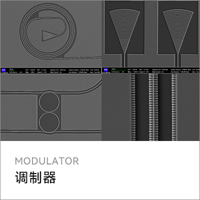
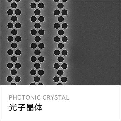
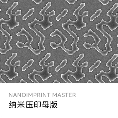
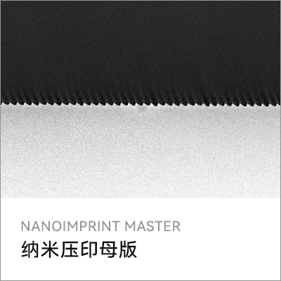
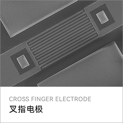

Lithography refers to any replication process that forms three-dimensional patterns on the surface of a substrate using photosensitive photoresist materials and controllable exposure, thereby transferring the patterns onto a flat surface. For the semiconductor manufacturing industry, lithography describes the process used to form extremely small feature patterns, which is of great importance in the fabrication of micro and nanostructures. Lithography is at the center of micro-nano processing and is often regarded as the most critical step in this field. Currently,
Lithography capabilities : ultraviolet exposure, electron beam exposure, laser direct writing exposure, and deep ultraviolet exposure.
The sizes of exposure substrates : 1cm*1cm, 2cm*2cm, 2 inches, 3 inches, 4 inches, 6 inches, 8 inches, 12 inches, etc.


